
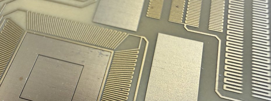
Wire bonding is an established bonding technique in the semiconductor industry and microelectronics. Whether high-quality, long-lasting bonds are formed depends crucially on the cleanliness of the bonding surfaces. The dry and scalable QuattroClean snow jet technology reliably and cost-effectively ensures the required cleanliness and can be automated as needed.
As a standard method for electrical contacting in assembly and interconnection technology, wire bonding has been established for 70 years across a broad spectrum of applications. It ranges from semiconductor technology, microelectronics, and optical components to automotive applications, consumer products, MEMS, and industrial sensors, as well as specialized applications such as the bonding of battery cells for electric mobility, rechargeable power tools, and energy storage systems. “Basically, wire bonding is divided into three major process groups. Two of these are fine-wire processes, in which—depending on the application—wires made of gold, silver, aluminum, or copper with a diameter of 18 to 50 µm are used. The third group involves thick-wire bonding with wire diameters ranging from 100 to 500 µm,” explains Stefan Schmitz, Managing Director of Bond-IQ GmbH. The consulting firm specializing in wire bonding technology is the initiator of the Surf:Guide industry project. The project’s goal is to develop guidelines on the cleanliness and condition of bond surfaces, which will serve as the basis for creating an internationally recognized, industry-standard.
Cleanliness—a key factor in quality
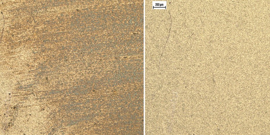
Since the formation of bonds in both thin-wire and thick-wire bonding occurs at the nanometer scale, the metals to be bonded must be brought within an atomic distance of one another. Accordingly, impurities or interlayers as thin as 5 to 10 nm can hinder the bonding process. These include, for example, fingerprints, bleeding adhesives, flux residues, outgassing from adhesives and other polymers, dust, oxides, or residues from wet-chemical cleaning processes in particular. “Visually detectable contamination is critical for bonding. If this contamination is no longer visible after cleaning, the bonding surface is normally sufficiently clean. This can usually be determined using a microscope and a visual before-and-after comparison. This alone can increase the success rate three- to fourfold,” explains Stefan Schmitz.
Method for Cleaning Bonding Surfaces
Traditionally, bonding surfaces are still cleaned using wet chemical processes with solvents or water-based media, which require energy-intensive drying. Plasma cleaning can be used for thin, known, and very specific types of contamination. Laser cleaning is another alternative. “For very sensitive surfaces, such as those in microelectronics, however, the costs of a laser system and the appropriate laser technology must first be balanced,” explains Stefan Schmitz. “The industry is currently showing interest in QuattroClean snow jet cleaning, as it can also remove more tenaciously adhering, encrusted contaminants.”
Dry, targeted, and sustainable cleaning
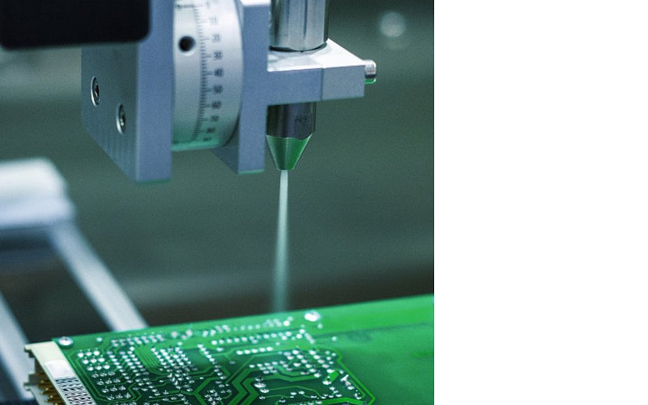
The scalable and cleanroom-compatible QuattroClean snow jet technology is a dry cleaning process for full-surface and localized applications. The process is suitable for the reproducible removal of particulate contaminants down to the submicrometer range and film-like contaminants down to the nanolayer level. QuattroClean technology uses liquid carbon dioxide—recycled and purified from chemical production processes and biomass energy generation—as its cleaning medium. It is channeled through a flexibly adjustable, wear-free dual-material annular nozzle and expands upon exit into fine snow crystals, which are bundled by a separate compressed-air jet and applied to the surface to be cleaned at supersonic speeds. The cleaning effect is based on a combination of thermal, mechanical, solvent, and sublimation effects. Since the crystalline carbon dioxide completely sublimates during the process, the treated surfaces remain dry. Removed contaminants are extracted along with the process gas, preventing recontamination of the surfaces and contamination of the surrounding area. In combination with process gas from Linde, the effective QuattroClean process holds the Green Screen certification for cleaners and degreasers from Clean Production Action.
Cleaning technology for a wide range of applications
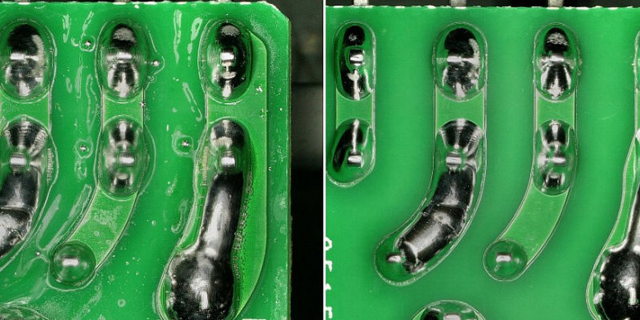
The low hardness of the fine snow crystals makes it possible to clean even very sensitive and finely structured surfaces. This opens up a very broad range of applications for QuattroClean snow blasting technology. Among other things, the process is used to remove flux and solder residues from PCBs and PCBs, to remove chemical and particulate contaminants from bond pads, and to clean battery cells prior to contacting. “The process can be used very efficiently on printed circuit boards, which often have a mixture of organic residues such as grease, fingerprints, flux, or residues from wet chemical cleaning processes. We have also achieved excellent results on semiconductors and on packages that have undergone electroplating or other wet chemical processes,” reports Stefan Schmitz. The relatively straightforward automation of the cleaning process—and its integration into production lines—also contributes to this. “This results in two advantages. First, automated cleaning ensures reproducible, consistent results. Second, when cleaning is integrated into the manufacturing process, fresh contaminants can be removed immediately before they become an even bigger problem due to storage processes,” adds Stefan Schmitz. (OM-11/26)
Contact
Acp Systems AG
Berblingerstraße 8
71254 Ditzingen (Germany)
Phone +49 (0)7156 / 48014 - 0
www.acp-systems.com
Acp Systems AG
Acp Systems AG is a global technology leader in the field of Advanced Clean Production, related process automation, and system integration, with its headquarters in Germany. Its core technologies include QuattroClean snow jet cleaning, micro-dosing, and intelligent handling solutions for flexible materials and films.