
Von Ardenne Expands HiPIMS Technology for Semiconductor Panel-Level Packaging
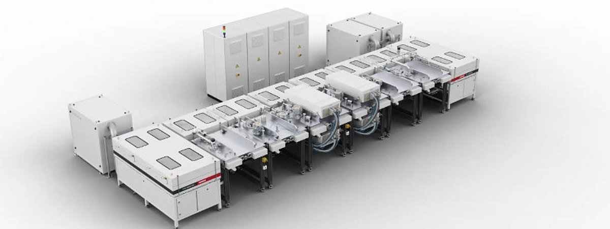
Von Ardenne, a provider of high-precision vacuum coating systems and jointly developed material solutions, is expanding its portfolio for semiconductor deposition to include panel-level packaging (PLP).
The new HiPIMS (High Power Impulse Magnetron Sputtering) solution deposits barrier and seed layers with a high aspect ratio in through-glass via (TGV) holes. This enables the production of dense, highly adhesive functional layers with improved material properties. The foundation for this is Von Ardenne’s modular horizontal coating platform, HISS, which is designed for large-area deposition and serves as a platform for the development and production of PLP processes. By using HiPIMS on the HISS system, the company is transferring the technology from the wafer level to the panel level. According to Von Ardenne, better adhesion and denser layers can help reduce rework, increase service life, and eliminate process steps in certain applications. The technology enables semiconductor manufacturers to transfer established deposition processes from 300-mm wafer formats to larger panel formats for advanced packaging applications. These include, among others, through-glass vias and redistribution layers (RDL).
HiPIMS Deposition for Panel-Level Packaging
With panel-level deposition, Von Ardenne aims to achieve higher manufacturing efficiency in the production of advanced semiconductor packages. A key challenge in the transition to larger substrates is meeting the requirements for uniformity and layer performance even across larger areas. The combination of a scalable equipment platform, substrate handling, and HiPIMS deposition is intended to create the technical conditions necessary for this. According to the Yole Group, the market for panel-level packaging is experiencing strong growth. By 2025, PLP is projected to generate revenue of more than $300 million. An average annual growth rate of more than 40 percent is projected for the next five years. High-end PLP applications for artificial intelligence and high-performance computing (HPC) are considered key growth drivers.
Contact details and information on the companies and institutions presented here can be found in our interactive surface technology industry directory.