Inkjet marking varnish from Peters conserves resources
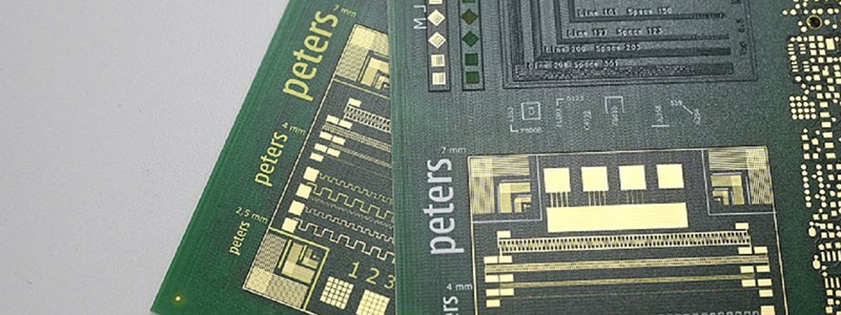
In addition to the inkjet solder resist, Peters will be presenting a white and a yellow inkjet marking resist at Productronica 2023. The marking print is used, for example, to display component positions and consecutive serial numbers on the solder resist.
The new marking lacquer from Peters Lacke is compatible with the Elpemer and Elpejet solder resists, ensuring good adhesion to the PCB. This should also be the case on solder resist masks from the competition. "The inkjet process conserves resources because a complex screen printing process does not have to be used for every PCB design," says Kevin Poth. The Elpepcd project manager developed the marking lacquer with his colleague, lacquer laboratory technician Jonas Sutman, in the Peters laboratory. As the inkjet process is a digital process, smaller margins can also be printed. "With the screen printing process, it only pays off from a certain quantity," emphasizes lacquer engineer Kevin Poth. At Productronica from November 14 to 17, 2023 in Munich, the Peters team led by Kevin Poth will be demonstrating the newly developed marking lacquers from the R&D department of the lacquer manufacturer from the Lower Rhine region. At stand B3-343 at the world's leading trade fair for the electronics manufacturing industry, the Peters specialists will be highlighting the advantages of inkjet marking varnish. In addition to the environmental aspect, the digital printing process can also be carried out more quickly and therefore saves costs. The bottom line: less waste, less energy consumption, economical use of a high-tech product.
In combination with the Elpejet IJ 2467 inkjet solder resist, for example, which plays a special leading role at the two Peters stands at Productronica, industrial customers can be provided with a perfect solution for reliable and durable solder resist and insulation coating and marking of the PCB. "The inkjet process is particularly advantageous for prototypes and very small quantities," says Kevin Poth. Another advantage: with the flexible inkjet process, solder resist and marking lacquer can be applied in a single process step. This is followed by joint final thermal curing at 150° Celsius for one hour. Kevin Poth: "This saves a considerable amount of energy as the process does not have to be repeated." The 31-year-old University of Applied Sciences Niederrhein graduate, who has been driving the inkjet methodology at Peters in Research & Development over the past seven years in the test facility on the inkjet printer, says: "As a digital printing variant, the process involves a particularly low use of material and waste. The advantages for customers in the PCB industry are obvious." The project manager also points out that each coated PCB can be individually labeled. "This makes them reliably identifiable and traceable."
Contact details and information on the companies and institutions presented here can be found in our interactive surface technology industry directory.