Fraunhofer IPMS analyzes contamination of wafer surfaces
The Fraunhofer Institute for Photonic Microsystems IPMS is expanding its analytical capabilities in the field of wafer contamination. Vapor phase decomposition in combination with mass spectrometry with inductively coupled plasma (VPD-ICP-MS) enables precise monitoring of wafer surface contamination.
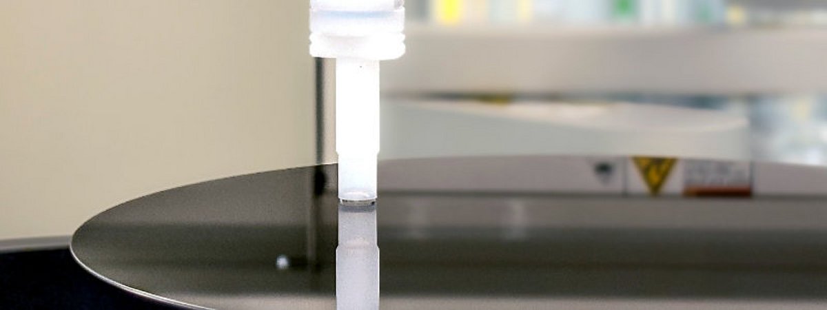
Wafers are thin, circular slices of semiconductor material that serve as the basis for the production of microchips and other electronic components. The quality and purity of the wafer surface are crucial for the functionality and performance of the end products. Various characterization methods are used to detect and quantify contamination. These have now been expanded at Fraunhofer IPMS to include ultra-trace element analysis. After etching 200 or 300 mm wafers with HF vapor (hydrofluoric acid), a drop is applied to the wafer surface and moved over it. The drop collects the soluble residues present on the surface and is then filled to a volume of 1 ml. The dissolved elements are then analyzed using inductively coupled plasma mass spectrometry (ICP-MS). This method provides precise quantitative information about the dissolved elements on the wafer surface.
Analytics for quality assurance on wafer surfaces
Ultra-trace element analysis offers comprehensive possibilities: For example, surface and bevel scans are performed to analyze 39 elements with RF scanning solution, which enables detailed characterization of the wafer surface. For special applications, aqua regia can also be used as a scanning solution for five precious metals. The laboratory is equipped with state-of-the-art equipment, including the VPD system Wafer Surface Preparation System WSPS2 from PVA Tepla and the iCap RQ mass spectrometer from Thermo Scientific. These technologies enable precise characterization and quality assurance in the semiconductor industry. With this expansion, Fraunhofer IPMS consolidates its position as a leading research institute in the field of 300 mm wafer processing and contributes to improving production quality in semiconductor manufacturing.
Contact details and information on the companies and institutions presented here can be found in our interactive surface technology industry directory.